
Contents
Hardware
For connecting the various components without the need for soldering, the use of so-called jumper-wires is recommended. Of course, also regular cables can be soldered onto the pin headers. For the optional Bluetooth Bee module, soldering unfortunately is inevitable because of the short pins and their small pitch.
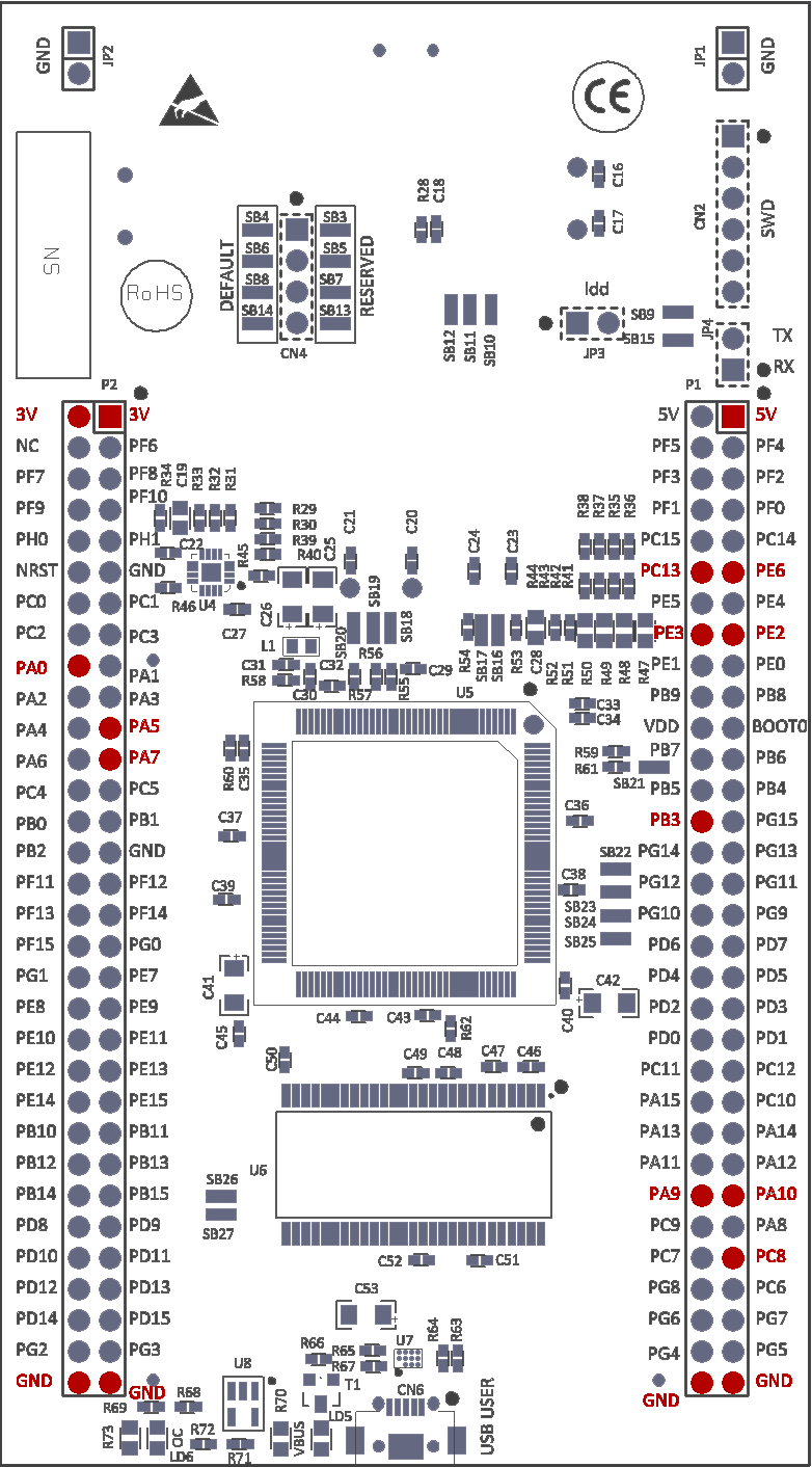
- The jumper-settings on the Discovery Board must be as follows:
CN4 – Both jumpers fitted (“DISCOVERY”-setting). This enables the onboard ST-LINK/V2 programmer/debugger to be used for our STM32 microcontroller. If the jumpers are not fitted, you can use the ST-LINK programmer for programming external microcontrollers.
JP3 – fitted. With this jumper, you can measure the current consumption of the microcontroller. Just remove it and insert a current measurement device instead.
JP1 and JP2 are fitted by default and can be kept like this. Both jumpers connect GND to GND and thus have no direct use. If you would require more ground pins – here you go! - Besides the jumpers, there are several solder bridges on the board that don’t need to be changed. Further information on their use can be found in the board’s User Manual.
- Now you can wire all components according to the following table:
Port / Pin Connection to
Connectors for rotary encoder (speed controller)
Bottom view of the board
PA5 Rotary encoder (speed controller) Channel A
PB3 Rotary encoder (speed controller) Channel B
PC13 Rotary encoder pushbutton (Select)
3V Rotary encoder supply voltage
GND Rotary encoder ground
PA0 External Emergency Stop button (optional) as alternative to the blue button on the board. The button must pull PA0 to VDD (3.3V). The internal Pull-Down resistor of the blue on-board button does the rest. For more information please consult the schematics or the User Manual.
LED Ring PE2 Sparkfun LED Ring CLK Pin or Seeed Studio Circular LED DCKI Pin PE3 Sparkfun LED Ring LATCH Pin PE6 Sparkfun LED Ring DAT Pin or Seeed Studio Circular LED DI Pin 3V Seeed Studio Circular LED Ring supply voltage
GND Seeed Studio Circular LED Ring ground
DCC signal output to input-optocoupler of a DCC booster
PC8 DCC signal to booster
PA7 DCC signal (complementary) to booster
GND DCC reference ground to booster
Bluetooth module for a wireless connection to an Android mobile device
PA9 Bluetooth Bee v2.0 Rx Pin PA10 Bluetooth Bee v2.0 Tx Pin GND Bluetooth Bee v2.0 GND Pin 3V Bluetooth Bee v2.0 3V3 Pin Connection of an external 5V power supply as alternative to USB power supply
GND External ground
5V External 5V power supply
Encoder-Interface
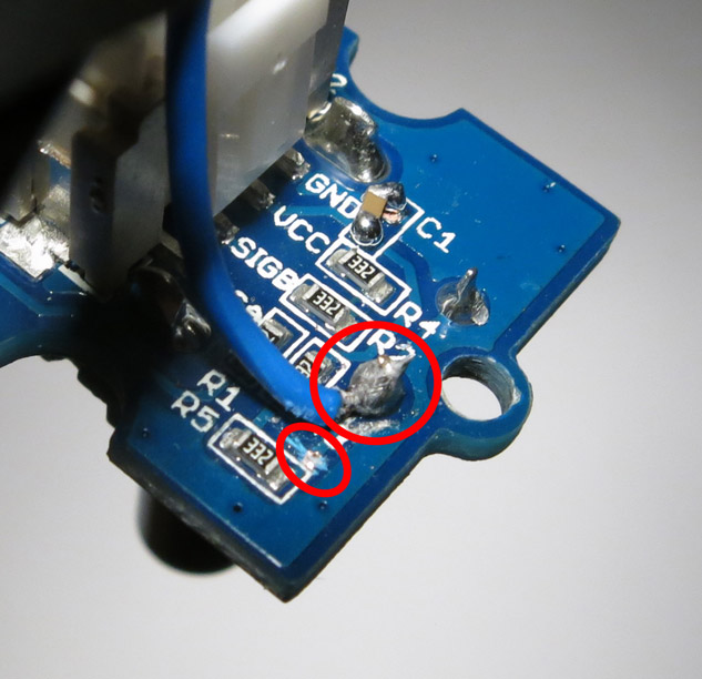
If you use the Seeed Studio Grove encoder, the signal of the encoder pushbutton unfortunately is not available on the 4-pole interface. The pushbutton also connects to GND instead of supply voltage level. Thus some minor modifications have to be done: a separate jumper cable must be soldered to the pushbutton pin at the encoder (to be able to connect it to PC13 on ARC1) and the circuit track to R5 must be opened, e.g. by cutting with a knife (see figure).
When using an arbitrary custom encoder (neither the Seeed Studio Grove encoder nor the Sparkfun Illuminated encoder), the encoder must switch its phases A and B against VDD (3V). Depending on whether the pushbutton switches to GND or to VDD, you have to choose between different ARC1 firmware versions:
ARC1 version for Seeed Studio: Encoder-Pushbutton switches to GND
ARC1 Version for Sparkfun: Encoder- Pushbutton switches to VDD (3V)
Booster-Interface
As there are many commercial and DIY boosters on the market / on the web and a booster would require a custom PCB layout, a booster is not (yet) part of the ARC project. A good list of boosters is given here, but also Google will give a bunch of good results for boosters. Also recommended are the boosters of the OpenDCC project.
ARC1 provides a differential 3.3V DCC signal on pins PC8 and PA7 (positive signal on PC8, negative signal on PA7). Any GND pin can be used as reference for the DCC signal. Thus ARC1 should be compatible with almost any available booster circuit.
Import for the selection and connection of a booster is the galvanic isolation between the booster and ARC1 (e.g. by use of an optocoupler). Most of the commercial and DIY boosters provide adequate means of galvanic isolation. The isolation is important, as in many cases the command station (e.g. ARC1) and the boosters are supplied by different power sources or are localized at different places and thus operate at a different ground level. If there is no galvanic isolation, equalizing currents on the DCC signal lines can permanently destroy your command station.
Software
A great advantage of the ST Microelectronics development boards is, that they are already equipped with an on-board programmer and you won’t need to buy or build a separate programmer for flashing the firmware to ARC1. ST’s proprietary programming and debugging interface is called ST-LINK/V2 or ST-LINK/V2-1 and uses the Mini-USB interface of the board.
Important note: For flashing the firmware, any external 5V power supply should be disconnected. While flashing, the board will get powered by USB.
- First of all, you need the ST-LINK USB driver. You can find it here: http://www.st.com/en/embedded-software/stsw-link009.html. Unfortunately you have to register on the ST website first.
- You will also need the STM32 ST-LINK utility for programming / flashing of ARC1 based on the compiled firmware binary files. You can download this tool after registering (of course you will only need one registration) here: http://www.st.com/en/embedded-software/stsw-link004.html.
- Connect the Mini-USB interface (NOT the Micro-USB interface next to the display) of the development board with your PC. After some seconds the demo-software of ST should appear on the LCD display.
- Double-check the correct jumper setting (see above).
- Run the STM32 ST-LINK utility and open the ARC-firmware file (*.hex) with “File->Open File” (STRG+O).
- Establish a connection to the development board with “Target->Connect”. If the USB driver was installed successfully, this should not evoke any problems. A successfully established connection should give the following log output:
16:40:44 : Connected via SWD.
16:40:44 : Connection mode: Normal.
16:40:44 : Debug in Low Power mode enabled.
16:40:44 : Device ID: 0x419
16:40:44 : Device flash Size: 2MBytes
16:40:44 : Device family: STM32F42xxx/F43xxx - After the connection is established, select “Target->Program & Verify” (STRG+P) and “Start” in the following dialog window to start the programming. You don’t need to change the settings.
- The programming and verification should take around 10-20 seconds. After it is completed successfully, the board should restart and boot into the ARC1 firmware. The log output should list something like this:
16:47:16 : Memory programmed in 12s and 293ms.
16:47:16 : Verification…OK
16:47:16 : Programmed memory Checksum: 0x015A31B9 - ARC1 is now ready for use and the ST-LINK utility can be closed. Sometimes a manual reset is required before the board starts into the firmware for the first time (reset by pressing the black reset button on the board or by shortly disconnecting the power supply).